欢迎光临~泰州巨纳新能源有限公司
语言选择:
 ∷
∷

∷
 ∷
∷
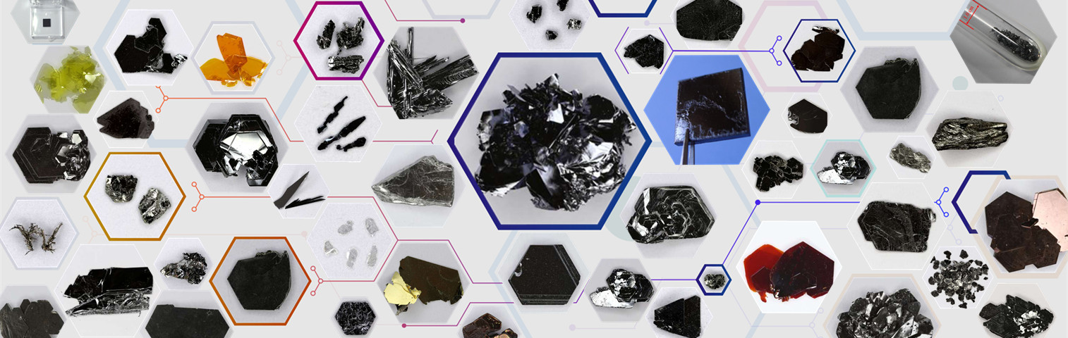
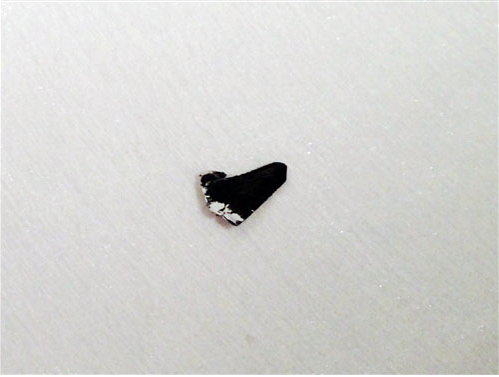
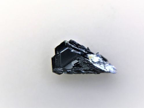
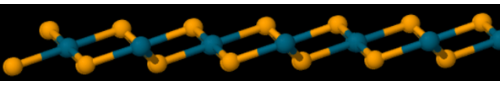
Bulk PdSe2 (palladium diselenide) has been predicted to exhivit 30 meV band gap which increases to 1.43 eV indirect gap (theoretical). In comparison to other TMDCs, PdSe2 has an uncommon structure: Pd atoms coordinate with four Se atoms, forming a square backbone lattice. It has also been recently shown that PdSe2 monolayer immediately undergo PdSe2 to Pd2Se3 crystal transformation. Owing to vast amount of Pd atoms, PdSe2 has been theoretically and experimentally shown to be catalytically active material thoigh fundamental research still remains at its seminal stages.
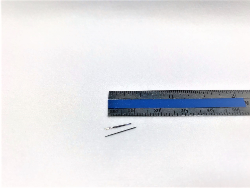
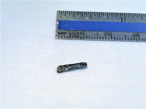
Growth method matters> Flux zone or CVT growth method? Contamination of halides and point defects in layered crystals are well known cause for their reduced electronic mobility, poor e-h recombination, low-PL emission, and lower optical absorption. Flux zone technique is a halide free technique used for synthesizing truly semiconductor grade vdW crystals. This method distinguishes itself from chemical vapor transport (CVT) technique in the following regard: CVT is a quick (~2 weeks) growth method but exhibits poor crystalline quality and the defect concentration reaches to 1E11 to 1E12 cm-2 range. In contrast, flux method takes long (~3 months) growth time, but ensures slow crystallization for perfect atomic structuring, and impurity free crystal growth with defect concentration as low as 1E9 - 1E10 cm-2. So if your research needs truly high quality crystals for optoelectronics, scanning tunneling microscopy, spectroscopy, and other projects that rely on defect free crystals, flux zone growth is ideal for you. If you need catalytic materials, the presence of defects typically helps. In such case CVT growth crystals are better suited for catalysis. During check out just state which type of growth process is preferred. Unless otherwise stated, 2Dsemiconductors ships Flux zone defect free crystals as a default choice.
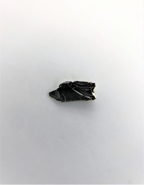
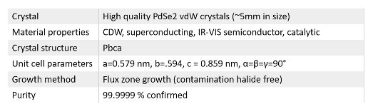
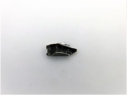
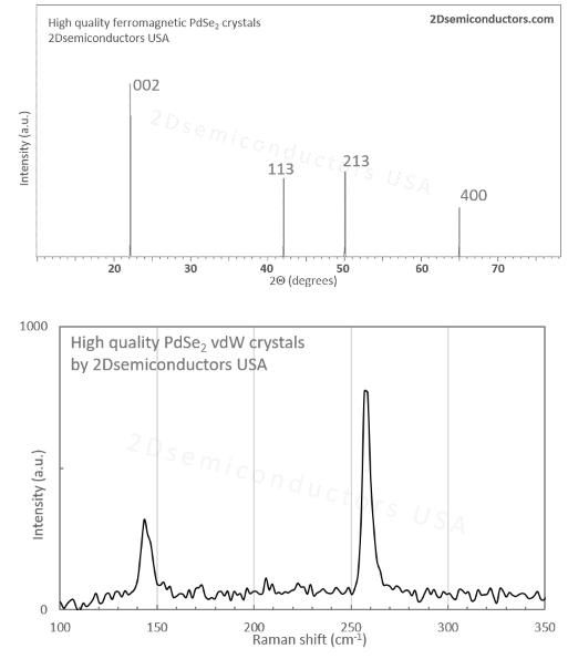
Properties of PdSe2 vdW crystals by 2Dsemiconductors USA

联系人:严春伟
手机:13914543285
电话:0523-86190619,86192878
邮箱:taizhou@sunano.com.cn
地址: 江苏省泰州市凤凰西路168号